A Beginner’s Guide to Understanding PCB Assembly Processes
Martin Huang
Posted on January 8, 2025
Printed Circuit Board Assembly (PCBA) is a crucial stage in the creation of electronic devices. It’s where the bare PCB is transformed into a functional component by mounting electronic components onto it. This process can seem complex to beginners, but understanding its basics can demystify the journey from design to a working product. In this guide, we’ll break down the key steps and technologies involved in PCBA.
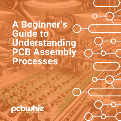
What Is PCB Assembly?
PCBA involves attaching and soldering electronic components to a printed circuit board to make it operational. This stage follows the PCB fabrication process, where the circuit design is etched or printed onto a substrate. The assembled PCBA is then tested to ensure it functions as intended.
Core PCBA Processes
1. Surface Mount Technology (SMT)
• Overview: SMT is the most common method for assembling components. It involves mounting components directly onto the surface of the PCB.
• Process:
1. Stencil Application: A solder paste stencil is placed over the PCB, and solder paste is applied to designated areas.
2. Pick-and-Place: Automated machines place components onto the solder paste.
3. Reflow Soldering: The PCB is heated in a reflow oven to melt the solder paste, securing the components.
• Advantages: Compact designs, faster assembly, and compatibility with high-volume production.
2. Through-Hole Technology (THT)
• Overview: THT involves inserting component leads through pre-drilled holes in the PCB and soldering them on the opposite side.
• Process:
1. Component Insertion: Components are manually or automatically inserted into the PCB holes.
2. Wave Soldering: The PCB is passed over a wave of molten solder to attach components.
• Advantages: Stronger mechanical bonds, ideal for high-stress environments.
3. Mixed Technology
• Many assemblies use a combination of SMT and THT to balance compact design with mechanical robustness.
Key Steps in the PCBA Process
1. Preparation and Inspection
Before assembly begins, the PCB and components are inspected for defects. Automated Optical Inspection (AOI) systems are often used to verify accuracy.
2. Component Placement
Precision is critical in placing components, especially in high-density designs. Modern pick-and-place machines can handle thousands of components per hour with remarkable accuracy.
3. Soldering
The soldering method depends on the assembly type:
• Reflow Soldering for SMT.
• Wave Soldering or Hand Soldering for THT.
4. Testing and Quality Control
After assembly, rigorous testing ensures functionality. Common methods include:
• In-Circuit Testing (ICT): Tests electrical performance of individual components.
• Functional Testing: Validates the assembled board’s overall performance.
5. Final Assembly
Once testing is complete, the PCBA may be integrated into the final product or sent to the customer for further use.
Challenges in PCBA
• Miniaturization: Smaller components require advanced equipment and techniques.
• Complex Designs: Multi-layer PCBs demand precise alignment and assembly.
• Quality Assurance: Ensuring reliability in every unit is critical, especially for mission-critical applications.
Final Thoughts
Understanding the PCBA process is essential for engineers, hobbyists, and businesses alike. With pcbwhiz, navigating this complex journey becomes seamless and efficient. Whether you’re prototyping a new design or scaling up for production, our services are designed to meet your needs with precision and reliability.
Keep Reading...
Introduction to PCB Surface Finishes: Why Are They Important?
Leiterplatten (PCBs) sind das Rückgrat moderner Elektronik und bieten mechanische

How to Upload Your BOM Using the BOM Importer
Richtlinien für das Format Ihrer Stückliste (BOM) Unterstützte Dateiformate Sie
Unleashing Creativity: How PCB Engineering Empowers Electronic Innovation
Kreativität treibt Innovationen an, und in der Welt der Elektronik

